
Taehee Kim: Meditation
Artist(s):
Title:
- Meditation
Exhibition:
Creation Year:
- 2004
Medium:
- Crystal Wafers, Polymer Plates, Chromium, Gold, Titanium, and Copper
Size:
- 2.8 feet x 8.8 feet
Category:
Artist Statement:
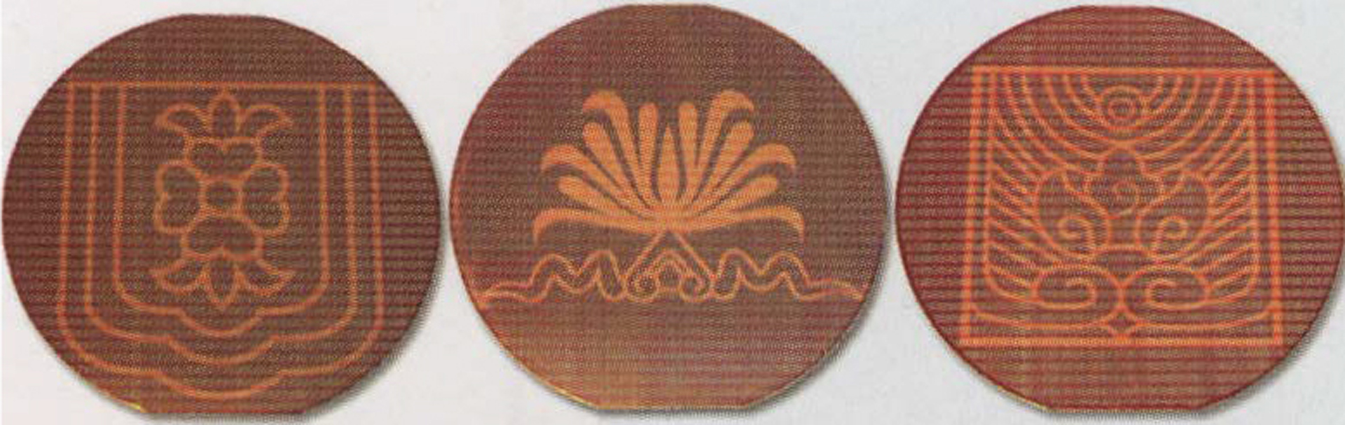
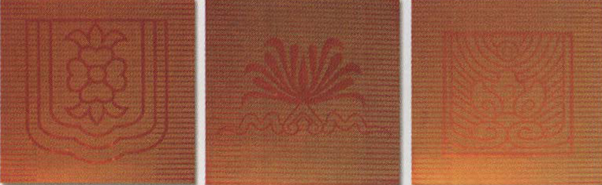
My body of work presents the concept of transcendence and spirituality in Eastern philosophy. It encompasses Eastern principles and spiritual meaning, showing parallels between the spiritual and the physical plane. My Buddhist experiences significantly influence my work because they have a strong emotional, spiritual, and intellectual effect on my life. Viewers may not receive my message directly, but it will challenge them to discover their own paths to the spiritual world in this moment in time. In this work, I used a pattern generator to experiment with the traditional lotus motif on semiconductor material. This image represents a transcendent path from the past to the present and from the material world to the spiritual world. I attempt to express new concepts of design that are transcendental dialogues beyond the appearance of the physical world. My belief is that art and science are ultimately one. One does not exist without the other; improvements in one reflect improvements in the other. The union of artistic idea and scientific exploration will bring new opportunities and knowledge, not only for art itself, but – through the integration of the two fields – a new insight
Technical Information:
Three different patterns of lotus motifs were impressed on silicon crystal wafers and polymer plates using scientific methods. The patterns were prepared by a pattern generator, which is used to make digitized patterns of circuits for semiconductor devices from AutoCAD. To transfer the images of the motifs, methods of semiconductor-device fabrication were employed, such as metal deposition using an electron-beam thermal evaporator, ultraviolet optical lithography, and metal etching. Patterns of data codes were overlaid consecutively on the transferred motifs. The deposited metals were chromium, gold, titanium, and/or copper with thicknesses several hundred times thinner than a sheet of paper. The process of ultra-violet optical lithography is similar to the process of photolithography and involved three steps: application of UV lightsensitive photo resists on top of deposited metals, exposure of UV lights to transfer patterns though digitized images of motifs or microbar codes, and development of exposed photo resists. Using metal etching chemicals, metal patterns of motifs were created along with the developed photo resist patterns. This project was supported by the Center for Advanced Microstructures & Devices at Louisiana State University. I would like to thank Dr. Josef Hormes and Dr. Jost Goettert for providing the resources and facilities.
Especially, I would like to express my gratitude to Yoonyoung Jin, Research Associate, for his extensive support and assistance.